
Arduino 引脚看着不少,项目一大就捉急:想控制 8 颗 LED,按老办法一个 IO 一颗,Uno 直接给你干到只剩俩口。这颗 74HC595 移位寄存器就是来解决这个事的——只用 3 个 IO 口,就能多出 8 个输出,而且还能级联继续翻倍。这次对照德州仪器 SN74HC595N 的数据手册,把接线、移位原理和代码一次说透。
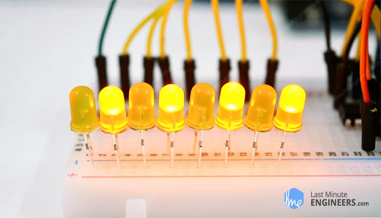
它凭什么用 3 个口控 8 颗灯
74HC595 是一颗典型的 SIPO 芯片(串入并出):串行收数据,并行出结果。它的对家 74HC165 是 PISO(并入串出),专门用来收集大量按键输入,俩方向刚好互补。
芯片内部其实有两组 8 位寄存器:一组叫移位寄存器,负责一位一位往里收数据;另一组叫存储寄存器,锁住数据再一次性送到 8 个输出脚。往 SER 脚送一个位、同时给 SRCLK 脚来一个脉冲,里面的所有位就整体往前挪一格,腾出位置给新位进来。打满 8 个脉冲,8 位就都进来了。
关键在第三脚 RCLK:数据进了移位寄存器不会马上出现在输出脚上,得等你给 RCLK 一个上升沿,把移位寄存器内容整批拷贝到存储寄存器,输出 QA 到 QH 才同时刷新。这个"先攒后放"的设计保证你装新数据的时候,输出保持稳定不闪。
引脚速查:16 个脚都在干嘛
市面上 74HC595 家家都在产,本文按最常见的 TI SN74HC595N(DIP-16 封装)讲,换别家前翻一眼数据手册确认差异。
- VCC(16 脚)接 5V,GND(8 脚)接地
- SER(14 脚)串行数据入口,位从 LSB 开始进
- SRCLK(11 脚)移位时钟,上升沿触发移位
- RCLK(12 脚)锁存时钟,上升沿把数据送上输出脚
- SRCLR(10 脚)清零脚,低电平有效,平时必须拉高
- OE(13 脚)输出使能,低电平有效:接地输出正常,拉高全部关断
- QA 到 QH 是 8 个并行输出,QH' 是串行出脚,专给级联用
接线:五步搞定
芯片插面包板,注意顶部 U 形凹口朝上,凹口左边就是 1 脚,两侧分跨面包板中缝。
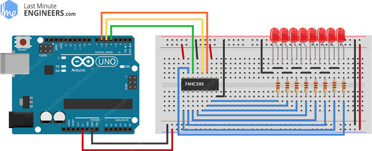
先供血:16 脚 VCC 和 10 脚 SRCLR 接 Arduino 5V,8 脚 GND 和 13 脚 OE 接 GND,让芯片处于正常工作模式。
再接三条控制线:11 脚 SRCLK 接 Arduino D6,12 脚 RCLK 接 D5,14 脚 SER 接 D4。这三根线就是"3 个 IO 控 8 路输出"的全部成本。
最后挂灯:每颗 LED 长脚(阳极)串一颗 220Ω 电阻接到 QA 到 QH,短脚统一接地。QA 对第一颗、QH 对最后一颗,接反了流水灯顺序就乱了。整体接线对照下图,照着插就行。
示例代码:流水灯
下面这段程序让 8 颗 LED 逐颗点亮,全亮后一起熄灭再循环。核心就是维护一个 byte 变量 leds 当"灯位图",bitSet() 置位,再交给 shiftOut() 搬运。
int latchPin = 5;  // Latch pin of 74HC595 is connected to Digital pin 5
int clockPin = 6;  // Clock pin of 74HC595 is connected to Digital pin 6
int dataPin = 4;   // Data pin of 74HC595 is connected to Digital pin 4

byte leds = 0;  // Variable to hold the pattern of which LEDs are currently turned on or off

void setup() {
  // Set all the pins of 74HC595 as OUTPUT
  pinMode(latchPin, OUTPUT);
  pinMode(dataPin, OUTPUT);
  pinMode(clockPin, OUTPUT);
}

void loop() {
  leds = 0;  // Initially turns all the LEDs off, by giving the variable 'leds' the value 0
  updateShiftRegister();
  delay(500);
  for (int i = 0; i < 8; i++)  // Turn all the LEDs ON one by one.
  {
    bitSet(leds, i);  // Set the bit that controls that LED in the variable 'leds'
    updateShiftRegister();
    delay(500);
  }
}

/*
 This function sets the latchPin to low, then calls the Arduino function 'shiftOut' to shift out contents of variable 'leds' in the shift register before putting the 'latchPin' high again.
 */
void updateShiftRegister() {
  digitalWrite(latchPin, LOW);
  shiftOut(dataPin, clockPin, LSBFIRST, leds);
  digitalWrite(latchPin, HIGH);
}
烧录逻辑三句话:updateShiftRegister() 先把 latchPin 拉低,用 shiftOut() 按位移出 leds 的内容,再拉高 latchPin 完成锁存。LSBFIRST 表示低位先走,正好对应 SER 脚"LSB 先进"的规矩。delay(500) 控制流水速度,改小就是快进。
进阶一:OE 脚做 PWM 调光
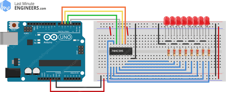
OE 脚接了 Arduino D3 这种 PWM 口,就能做整体调光。OE 是低电平有效,所以亮度值要反过来写:analogWrite 里给 255 减去亮度,亮度越低占空比越高。完整程序如下:
int latchPin = 5;         // Latch pin of 74HC595 is connected to Digital pin 5
int clockPin = 6;         // Clock pin of 74HC595 is connected to Digital pin 6
int dataPin = 4;          // Data pin of 74HC595 is connected to Digital pin 4
int outputEnablePin = 3;  // OE pin of 74HC595 is connected to PWM pin 3

byte leds = 0;  // Variable to hold the pattern of which LEDs are currently turned on or off

void setup() {
  // Set all the pins of 74HC595 as OUTPUT
  pinMode(latchPin, OUTPUT);
  pinMode(dataPin, OUTPUT);
  pinMode(clockPin, OUTPUT);
  pinMode(outputEnablePin, OUTPUT);
}

void loop() {
  setBrightness(255);
  leds = 0;  // Initially turns all the LEDs off, by giving the variable 'leds' the value 0
  updateShiftRegister();
  delay(500);

  // Turn all the LEDs ON one by one.
  for (int i = 0; i < 8; i++) {
    bitSet(leds, i);  // Set the bit that controls that LED in the variable 'leds'
    updateShiftRegister();
    delay(500);
  }

  // Gradually fade all the LEDs back to off
  for (byte b = 255; b > 0; b--) {
    setBrightness(b);
    delay(50);
  }
}

/*
 This function sets the latchPin to low, then calls the Arduino function 'shiftOut' to shift out contents of variable 'leds' in the shift register before putting the 'latchPin' high again.
 */
void updateShiftRegister() {
  digitalWrite(latchPin, LOW);
  shiftOut(dataPin, clockPin, LSBFIRST, leds);
  digitalWrite(latchPin, HIGH);
}

/*
 This function generates a PWM signal and writes it to the OE pin.
 */
void setBrightness(byte brightness)  // 0 to 255
{
  analogWrite(outputEnablePin, 255 - brightness);
}
这段的效果是流水灯逐颗点亮,全亮后整排渐暗熄灭,循环往复。接线只需在原电路基础上把 OE 从 GND 挪到 D3,对照下图即可。
进阶二:级联,3 个口变 16 个甚至更多
一颗 595 管 8 路,两颗呢?把第一颗的 QH' 串行出脚接到第二颗的 SER,两颗共用同一组 SRCLK 和 RCLK,就凑成 16 路输出的整体。想再扩就继续往下挂,控制脚始终只要那 3 个——代价只是移位时钟数翻倍,速度完全够 LED 用。
当初"16 颗 LED 要 16 个 IO"的难题,两颗 595 加 3 个 IO 就终结了。做数码管驱动、点阵屏、继电器组这类多路输出的活儿,这套思路照搬不误。
总结
74HC595 的本质就是"串行省线、锁存保稳":三个 IO 负责喂数据和发令,8 个输出各干各的。新手最容易翻车的两处——SRCLR 忘了拉高、QA 到 QH 接灯顺序反了——检查清单里都给你标了。跑通这版流水灯之后,级联和 PWM 调光都只是顺手的活,建议都试一遍。




讲道理,OE 低电平有效这个点是我当年自己烧了两颗才悟出来的。当时 OE 悬空没接,输出全关,还以为是芯片坏了买了三颗新的……文章里要是能再加一句『OE 千万别悬空』就完美了。另外 LSBFIRST 和硬件 LSB 先进对应的这段讲得清楚,很多教程都不解释 shiftOut 第三个参数干嘛的。
正好手头两颗595,晚上回去试试级联16路,谢谢老哥
问个小白问题:SRCLR 拉高的 5V 是直接并到 VCC 那根线上就行吗?面包板走线有点挤
QA 对第一颗 QH 对最后一颗这句太关键了,我上次接反顺序全乱还以为代码错了
PWM 那个 255-brightness 的反向写法解释得明白,比只会说'analogWrite 就完事'的教程强多了